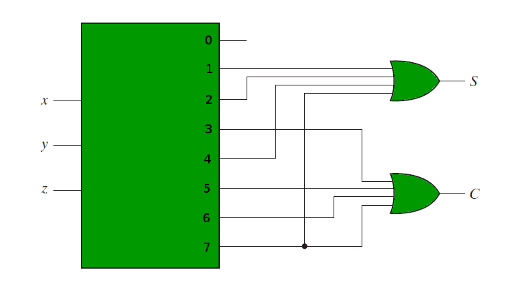
4 5 design a combinational circuit with three inputs x y and z and three outputs a b and c.
Design a combinational circuit with four inputs.
The inputs are d3 do and the output goes to the blanking input of the 7447.
This project is individual assignment no groups is allowed operation 1.
When the binary input is 4 5 6 or 7 the binary output is one less than the input.
Design a combinational circuit that will take 4 bits in binary as input and switch the first and last digits.
When the binary input is 0 1 2 or 3 the binary output is one greater than the input.
A combinational circuit can have an n number of inputs and m number of outputs.
The output s of combinational circuit depends on the combination of present inputs.
Each combination of input variables will affect the output s.
Solution for design a combinational circuit with 4 inputs a3 a2 a1 a0.
Design procedure of combinational circuits.
Control bits 0 1 operation design combinational circuit with 4 bits inputs design a 4 bits adder table 1.
The previous state of input does not have any effect on the present state of the circuit.
A block diagram of the combinational circuit is shown connected to the decoder display circuit in the following figure.
In this lesson we will design a combinational circuit for a light switch in which the light bulb comes on anytime there is an input of a prime number between 0 and 10 in the.
And three outputs x y z.
Eg 2 10 3.
We re going to elaborate few important combinational circuits as follows.
Half adder is a combinational logic circuit with two inputs and two outputs.
The inputs represent a binary number in the range.
The circuit must output o when the inputs are 1010 1111 and a 1 for all other.
Design a combinational circuit with 4 inputs and one output.
Design a circuit that has a 3 bit binary input and a single output that output 1 if it is a prime number.
This combinational circuit has n input variables and m outputs.
Combinational logic circuit design.
System functionality 1 2 note.